 By Marcus Linderoth, Thingsquare VP of Engineering
Inside each connected product is a piece of hardware. This hardware typically has to be custom designed for each product, but the level of customization varies depending on the product.
Designing hardware for a Thingsquare-compatible product is straightforward because there are ready-made reference designs to use as a starting point.
Supported Wireless Chips
Each wireless hardware design is is based on a wireless System-on-a-Chip (SoC) or combination of wireless chips. The Thingsquare platform currently supports a range of wireless chips produced by Texas Instruments.
Thingsquare supports the following chips in the CC13xx / CC26xx family, all 128 kB flash and 20 kB RAM variants:
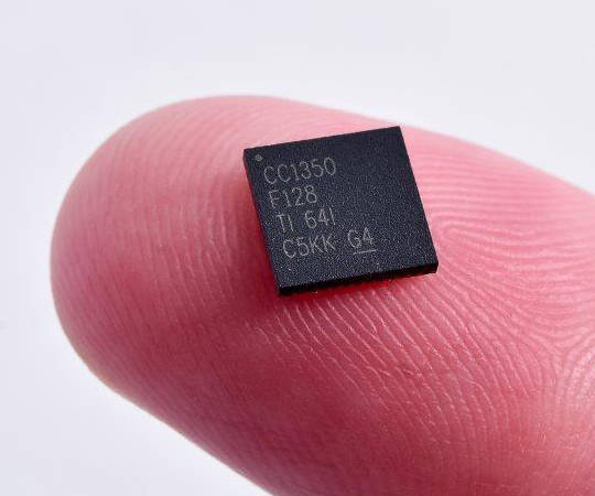
The TI CC1350 System-on-a-Chip.
- CC1310 rev B sub-GHz
- RGZ package with 30 GPIOs
- RHB package with 15 GPIOs
- RSM package with 10 GPIOs
- CC1350 sub-GHz, with BLE beacon support
- RGZ package with 30 GPIOs
- RHB package with 15 GPIOs
- RSM package with 10 GPIOs
- CC2650 2.4 GHz, with BLE beacon support
- RGZ package with 31 GPIOs
- RHB package with 15 GPIOs
- RSM package with 10 GPIOs
Thingsquare supports the CC2538 chip (2.4 GHz) in the 512kB variant.
We also support the combination of a CC2538 with a CC1200, for sub-GHz applications where flash space of the CC13xx-family is not enough.
For questions on other chips or combinations, please contact us.
Buy or Design?
Designing high-frequency radio hardware comes with a particular set of challenges that can be hard to nail down. Using a module is a convenient shortcut to save time and risk, since the RF parts are already designed and tested. The module must still follow the guidelines though (eg crystal oscillators), and you may need to add an external flash in the rest of the design.
The product owner typically must consider the cost-benefit trade-off in this decision. Generally speaking, when manufacturing in low volume, it makes sense to buy modules from a 3rd party vendor. When volume increases, it might start making sense to design the RF parts yourself, either as a one-off, or designing a module.
Third-party Modules
Third-party modules are typically designed according to the reference design by vendors with a high degree of expertise in RF. Many come with integrated PCB- or chip-antenna, making the rest of the hardware design a breeze. Examples of modules include the CC2650Moda.
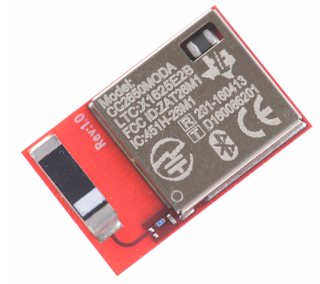
The CC2650MODA is a 2.4 GHz radio module based on CC2650 and a chip antenna.
Pros
- Pre-certified, meaning lower risk of failing certification
- Shorter time to market due to simpler hardware design
- Lower risk
Cons
- More expensive per unit
- Dependence on another party for supplies and long-term support
One-off Designs
This is when you design hardware that is fully integrated. All components, antennas, traces, etc are located on one single PCB.
Pros
- Lower cost per unit in volume
Cons
- RF design can be hard and take a lot of time
- Can’t re-use the design certifications in another product
Designing Your own Module
If you plan on releasing more than one product, it might be beneficial to design a radio module yourself. That way, you design and certify the module itself, which is then incorporated in the designs of the products.
For example, if you want to sell a light sensor product, a lamp product, and a light switch product, it is better to design and certify a radio module, which is then used in all the products. That way, the certification of the products is simplified and thus cheaper.
Pros
- Lowest cost per unit in volume, over a product line
- Certification and ev Bluetooth listing can be re-used across products
Cons
- RF design can be hard and take a lot of time
Wireless Hardware Design and Regulations
For wireless electronics, there are several regulations that must be met. To be able to meet these regulations, there are a number of hardware design details that must be be paid extra attention to:
- Substrate (material, thickness).
- Copper layer(-s) thickness.
- Signal trace dimensions, form, shape.
- Ground planes, decoupling, vias.
- High and low frequency crystal oscillators.
This is important since errors may result in failing regulations due to spurious emissions, worse RF performance due to impedance mismatch, and otherwise hard to debug errors due to EMI or clock glitches.
The crystal oscillators must have the same specification as in the reference design, with the same nominal frequency and accuracy (typically expressed in ppm) across the temperature range. This goes for both low (typically 32.768 kHz) and high (commonly 24 MHz) frequency oscillators. You must use external crystal oscillators for both low and high frequency, not the internal oscillators.
Using a reference design in a good way to avoid problems with regulatory requirements.
Reference Designs
There are reference designs available for free and without any associated royalty costs (subject to the respective owners) from the device manufacturers. See the respective manufacturer for up to date rules and conditions. Follow the links below to find design documents on the following reference designs.
Based on the Texas Instruments Launchpad
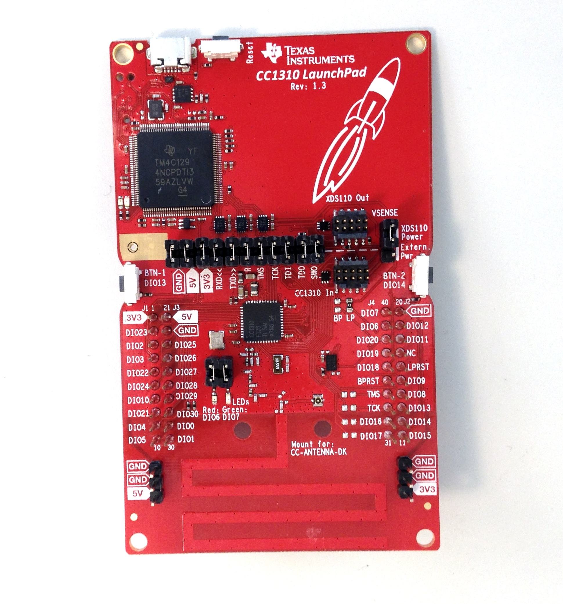
The Texas Instruments Launchpad reference design.
Based on the CC1310 Launchpad
The CC1310 Launchpad has a differential antenna output, by default routed to the PCB antenna. By changing a couple of SMD components in the signal path, it routes the signal to a Hirose U.FL connector instead.
Based on the CC1350 Launchpad
Same as the CC1310 Launchpad, but the CC1350 Launchpad has also a 2.4 GHz PCB antenna for BLE functionality. The antenna output is also differential, with an external RF switch to select the antenna path.
Based on the CC2650 Launchpad
Similar to the CC1310 Launchpad, but CC2650 Launchpad has a 2.4 GHz antenna instead.
Based on the Texas Instruments Sensortag
Based on the CC2650 Sensortag
The stk">CC2650 Sensortag is very similar to the CC2650 Launchpad, but adds a number of sensors.
Based on the CC1350 Sensortag
The stk">CC1350 Sensortag is very similar to the CC2650 Sensortag, but it has a sub-GHz antenna, and a 2.4 GHz antenna. In contrast to the CC1350 Launchpad, this design has single-ended antenna outputs, one for the sub-GHz antenna, one for the 2.4 GHz antenna, and no antenna switch. This makes for a smaller BOM cost and lower power consumption, at the price of lower range (the reduction is on the order of 3 dB).
Based on the CC2538EM
The CC2538EM is a bare-bones reference design.
Based on the CC2538 em and the CC1200
Combination of the CC2538em and CC1200em sub-GHz radio transceiver.
Preferably, follow the pinout as follows,
CC1200      CC2538
SPI CLK     PB2
SPI MOSI    PB1
SPI MISO    PB3
SPI CS      PB5
GPIO0       PB4
RESET       PC7
Hardware Components
RF Components
We strongly recommend to think about the antenna from the start of the design. This is a trade-off, like everything else. Design, enclosure, environment, cost, size, performance, COTS availability factors in. A certification may be bound to using a specific antenna too, creating a dependence on availability of the antenna.
PCB Antenna
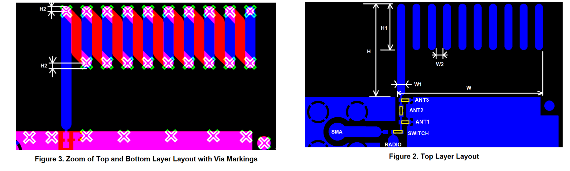
The TI Launchpad, TI 2.4 GHz Sensortag, and TI sub-GHz Sensortag use PCB antennas. Ie, the antenna is a printed directly on the PCB as part of the copper layer. This kind of antenna is inexpensive and simple. It does have a limited radiation pattern and limited range but price/performance is very good. Even very slight dimension changes, or not following the guidelines regarding ground plane and via stitching, will affect performance so follow the reference design with great care.
The Texas Instruments Sensortags show three different PCB antennas. First, the CC1350 Sensortag has a “Small Size 2.4 GHz PCB antenna”, together with a “Miniature Helical PCB Antenna”. The CC2650 Sensortag has a inverted-F antenna.
There are many antenna designs available. Dimensions and other important factors are found in the application note respectively.
Chip Antenna
Chip antennas are SMD components that uses a smaller PCB area than a PCB antenna, at a higher BOM cost. Chip antennas are supported too, follow directions for the SOC in use and the chip antenna to design a matching network of supporing components.
Externally Mounted Antenna
Many products - especially the ones less likely to end up prominently featured in peoples homes - feature a whip antenna. A whip antenna is basically a length of wire molded inside plastic. It takes up more space and costs more, but can be easier to design for, and has in general better performance than PCB or chip antennas.
Similarly, externally mounted antennas (eg using U.FL mounts, or regular SMA antenna connectors) are also supported. There are reference designs and application notes on this too.
RF Switch
The CC1350 supports both sub-GHz and 2.4 GHz operation (BLE beacons). The best range is achieved through using a RF switch and differential antenna output. For what RF switch to use, refer to Texas Instruments on a compatible RF switch. The CC1350 Launchpad reference design uses a Murata XMSSJE3G0PA-003 antenna switch.
By default, all CC1350 platforms assume an RF switch with the following default pins,
rf switch     CC1350
power         IOID_30
select        IOID_1
The power pin is for providing power to the switch, and select to select antenna path. The power pin is optional and does not have to be in use. If the target hardware does not have an RF switch, the user application has to override this by providing an empty void init_radio(void); function.
External LNA, PA
To extend range, a product can incorporate external power amplifier (PA) and/or low noise amplifier (LNA). This can be configured in customer application on bootup. Contact us for more information.
External Flash
In order to accomodate firmware updates over the air (FOTA), hardware building on CC13xx or CC26xx hardware must have an external flash chip. We support two main kinds: Macronix and Winbond. The storage area should be at least 512 kB large, but since the cost difference is very small, larger ones are preferred for flexibility reasons.
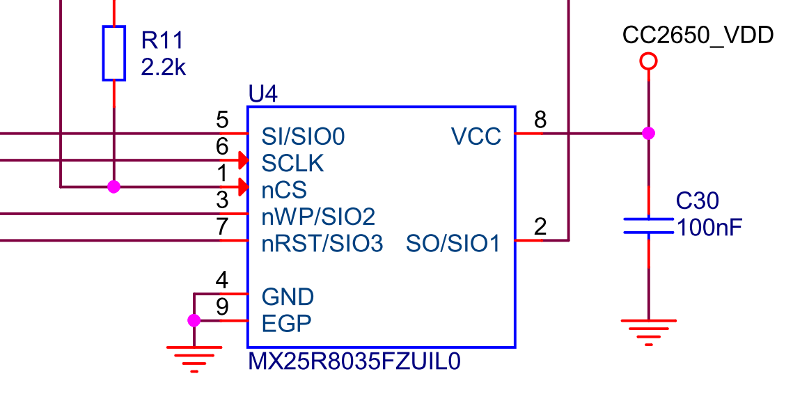
Macronix
Macronix external flash chips are preferred since they have lower steady-state power consumption than Winbond. The Launchpad and (newer) Sensortag reference designs make use of the MX25R8035FZUIL0 chip. The package is of no importance to the system, only that the command set is the same, and factors such as sector size etc.
Winbond
Old CC2650 sensortag designs use the Winbond W25X40CLUXI chip. It has slightly higher power consumption than the Macronix. Base new designs on the Macronix chip per above.
SPI Pinout
The pins used for the SPI communication with the external flash chip is configurable. The default pins are,
flash          CC13xx/CC26xx
SPI CLK        IOID_10
SPI CS         IOID_20
SPI MISO       IOID_8
SPI MOSI       IOID_9
Gateway Designs
The system supports two kinds of gateways: an Ethernet-based gateway, and a serial gateway.
Serial Gateway
A serial gateway uses a serial port to communicate with a host, eg a SBC. To connect the two, UART RX and UART TX has to be connected. By default, the following pinout is used,
host function       CC13xx/CC26xx function and pin
UART RX             UART TX IOID_3
UART TX             UART RX IOID_2
Ethernet Gateway
The Ethernet gateway uses an Microchip ENC28J60 ethernet chip. It can be used in combination with all the supported SOCs. By default, the following pinout is used,
enc28j60       CC13xx/CC26xx
SPI CLK        IOID_21
SPI CS         IOID_1
SPI MISO       IOID_12
SPI MOSI       IOID_15

enc28j60       CC2538
SPI CLK        PA2
SPI CS         PD5
SPI MISO       PA4
SPI MOSI       PA5
Other Components and Guidelines
Buttons
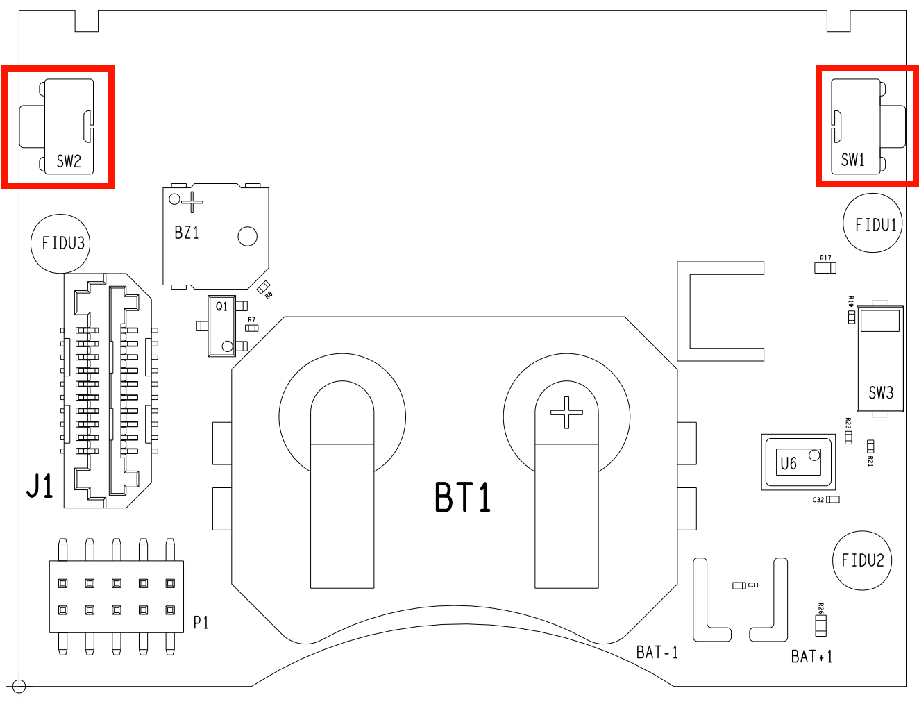
Reset Button
Including a reset button is always good, at least during the development phase. We suggest that if you leave out the reset button in production, you must ensure the reset line is strongly held so that no unintentional reset on the system is caused by EMI.
User Button
User buttons are not necessary as far as the system goes. You may add such for user-interfacing activities though.
UART Serial Output
We strongly advise to include a way to get UART debugging information out. The design does not have to include a UART-to-USB chip (such as FTDI or CP2102 or CH340G), but can just have test points or pin headers to attach to. UART can be configured on bootup. The default pinout is,
UART    CC13xx/CC26xx
RX      IOID_2
TX      IOID_3
CTS     not used
RTS     not used

default settings: 115200/8/n/1
LEDs
Power LED
Feel free to include a LED to indicate when power is applied, if the product so needs to. This can also be a helpful during development and can be left unpopulated in production.
Status LEDs
The system has APIs and support for a red, a green, and a blue LED. Which ones are present, their pins, and whether they are active high or low (CC13xx/CC26xx only) are configurable. All such LEDs must use the same high or low convention. You need to take the LED current into consideration when designing since too much current routed through the SOC might damage it.
The defaults are,
LED     CC13xx/CC26xx
Red     IOID_6
Green   IOID_7
Blue    IOID_UNUSED

active high by default
Other LEDs
LEDs for eg Lighting applications are typically driven with a customer-specific driver for this purpose, and as such is not limited to the API or conventions.
JTAG Programming Header
Unless you buy pre-programmed SOCs, you need to have a way to program the device during manufacturing. This is done over the JTAG interface. For simplicity, we suggest using the standard JTAG 2-by-5 pin connector with 1.27 mm pitch. Include a footprint for a male pin header, or receptables for pogo-pin fixture.
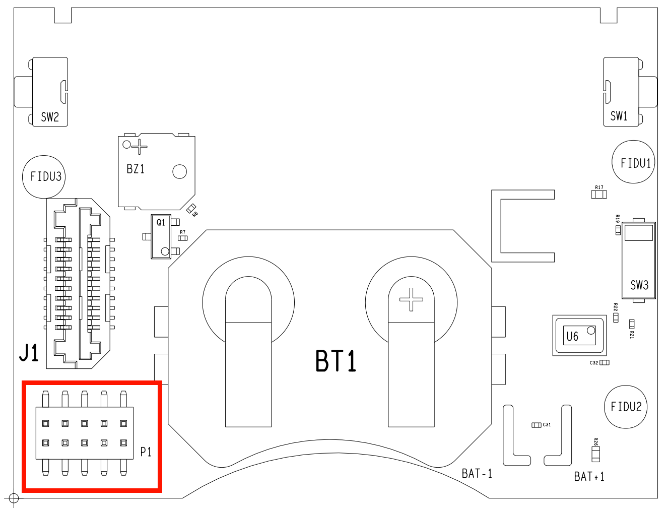
The firmware locks down all debug and programming interfaces. To reprogram the device after flashing with a Thingsquare firmware image, you need to perform a full erase before being able to program it again. This can only be done over the JTAG interface.
Regarding JTAG, do make sure that it is not susceptible to reasonable EMI. Refer to the CC13xx/CC26xx technical reference manual, sections 5.4 and 5.6.
Test Points
In case of small pitch components, or pads hard to reach with a probe, do consider adding test points for debugging.